Agentic PCB editor
November 5, 2026
A printed circuit board (PCB) holds electronic parts on a rigid insulating plate and connects their pins with flat copper tracks etched into the surface. Moving a circuit from a schematic to a board means choosing a board outline and a layer stack, placing footprints so their connections rarely cross, routing copper tracks of the right width, pouring ground planes, and checking that every track clears its neighbours before sending the files to a fabrication house.
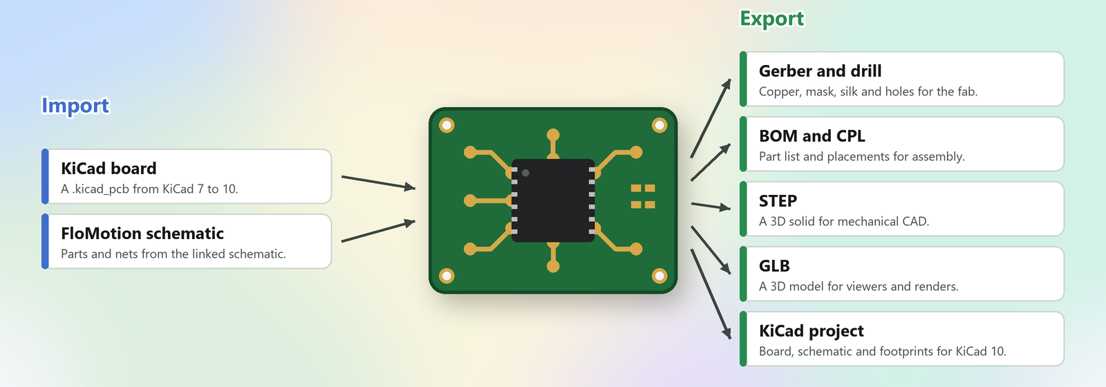
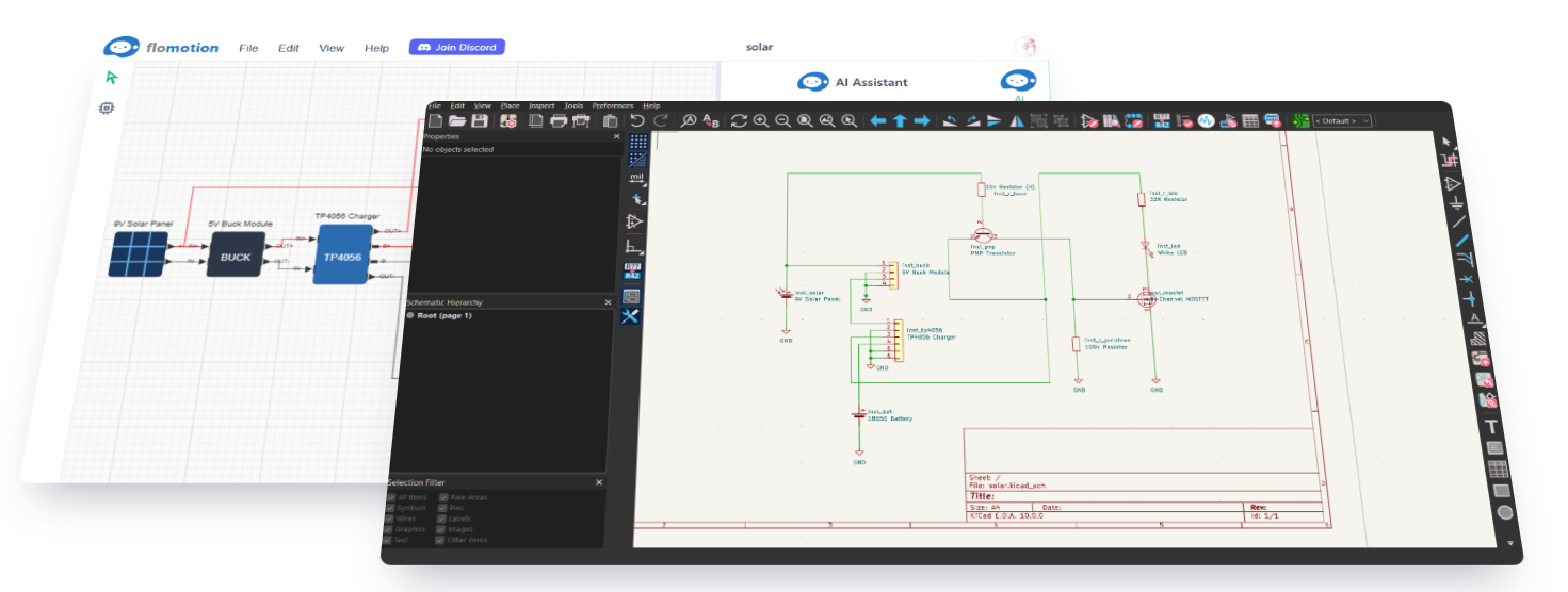
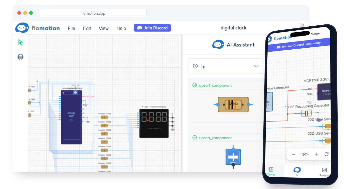
In FloMotion, the PCB editor opens in the browser on a desktop, phone or tablet and works directly on a KiCad 10 board file. It converts a schematic from the same project into an unrouted board, supports two to 32 copper layers, checks the layout against the schematic and the fabrication rules after every change, renders the board in 3D, and builds a bill of materials for assembly.
An AI agent sits beside the canvas and works on the same board as the manual tools. The agent can create the board from a prompt, place footprints, route nets, add ground pours and keepouts, run KiCad's design rule check on the server, draw missing 3D part models, and fix the issues that the checks report. Because the file is a standard KiCad 10 board, layout work can also move back and forth between the browser, desktop KiCad and the agent.
Why robot circuits move to a board
Robot electronics usually start on a solderless breadboard. A microcontroller development board, a couple of motor or servo drivers, an inertial sensor and a power regulator sit in spring clips linked by push-in jumper wires. That arrangement is quick to rewire on the bench, where nothing moves, while pin assignments and part values are still changing.
Once the circuit goes onto a moving frame, the breadboard starts to fail. Stepping motors, gearboxes and wheels vibrate the chassis and shake jumper wires loose in their clips. Servos and drive motors draw spikes of current through thin jumpers whose contact resistance drops voltage and resets the microcontroller. Long wire loops between the driver and the controller pick up switching noise and corrupt sensor readings, and a tangle of jumpers has no mounting holes to screw into a bracket.
A printed circuit board replaces the spring clips and jumpers with soldered pads and etched copper. Parts sit flat against a fibreglass core and their leads are soldered into plated holes or onto surface pads, so vibration cannot work them loose. Power for motors and servos runs along wide copper tracks over a continuous ground pour on the opposite side of the board, keeping loop areas small and voltage drops low. Mounting holes in the corners bolt the board straight to the robot frame, and once the layout is saved, a fabrication house can make a spare board or outfits for a second robot from the same file.
From schematic to board outline
A board layout starts from a finished schematic in the same project. Every symbol in the schematic already carries a footprint name and a list of nets that join its pins. Turning that schematic into a board means picking a board size, a corner radius and a number of copper layers, either in the new-board dialog or by asking the agent in plain words, such as a 60 by 40 millimetre four-layer board from the servo schematic. Boards can have from 2 to 32 copper layers, with each inner layer set up as a signal layer, a ground plane or a power plane.
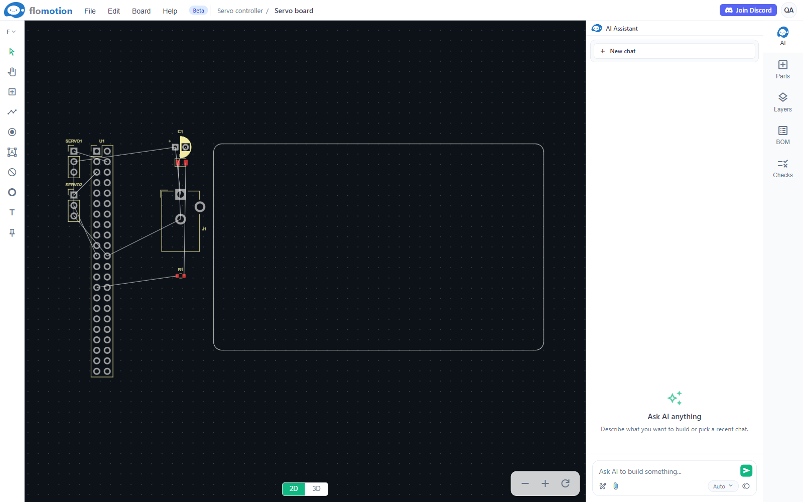
When the board first opens, the board outline is empty and the footprints from the schematic sit lined up to one side. Thin straight lines called the ratsnest stretch between pads that belong to the same net, showing every connection that still has to be routed in copper. The example in the image is a small servo controller with headers for an ESP32-S3 development board, two servo connectors, a barrel jack for power, a capacitor and an LED.
Placing parts and routing copper
Laying out the board happens in two stages: placing the footprints inside the board outline so related parts sit together and the ratsnest lines untangle, then replacing each ratsnest line with a copper track of a suitable width and pouring copper zones for ground or power.
Both steps can be done by hand in the browser, in desktop KiCad, or by the agent. In the browser, footprints drag into place, tracks draw between pads, and a note can be pinned to a spot on the canvas (for example, asking to move a decoupling capacitor closer to a connector) so the agent knows which area and part the note refers to. When asked to lay out a board on its own, the agent places the parts, routes the nets, adds ground pours and keepout areas, refills the pours, runs the board checks and fixes the violations they report. When the nets will not route cleanly in the available space, the agent suggests either a larger board outline or more copper layers rather than forcing tracks through tight clearances, since both choices change the fabrication price.
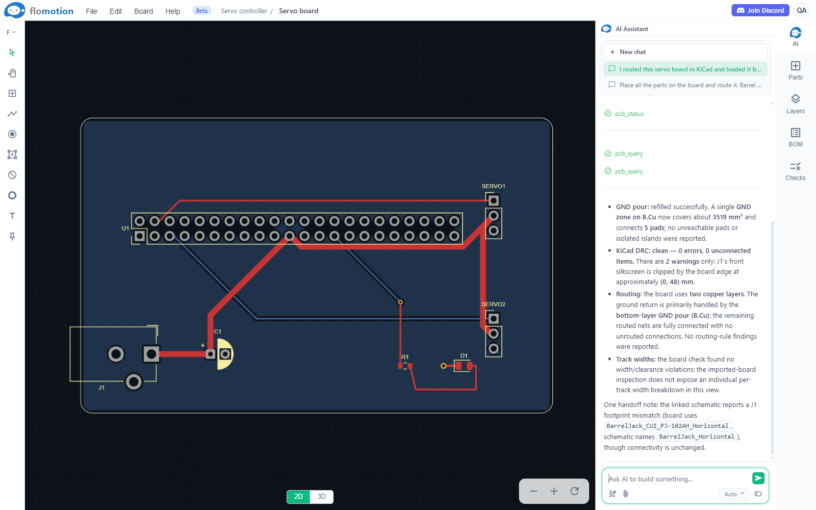
Because the project stores a native KiCad 10 .kicad_pcb file, the board round-trips with desktop KiCad without translation. A board can be started by the agent and finished by hand, or routed in KiCad and brought back for the agent to check and clean up. The servo board shown above was routed on two layers in desktop KiCad, with signal and power tracks in red on the top layer, and then loaded back into the browser editor. From there, the agent refilled the bottom ground pour and ran the design rule check to verify the layout.
Design rule and schematic checks
A routed board has to match the schematic and obey the physical limits of the fabrication process: tracks cannot touch tracks on other nets, copper must stay back from the board edge and out of keepouts, and every net must be completely connected. The editor runs its own board checker after every edit and also runs KiCad's own design rule check (DRC) on the server, using the same engine as desktop KiCad.
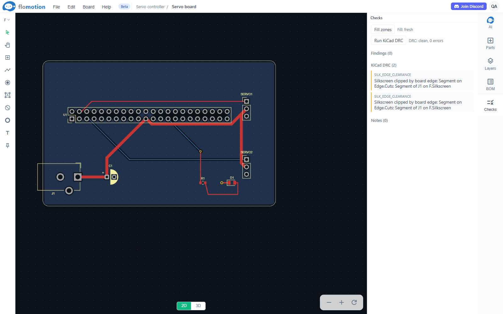
The Checks panel groups the results:
- Board geometry and copper rules: track-to-track and pad clearances, short circuits between nets, minimum track width, copper extending outside the board edge or inside a keepout zone, and isolated islands in copper pours.
- Connectivity and footprint overlap: unrouted ratsnest connections, pads left unconnected, and footprints whose courtyards or bodies overlap on the same side of the board.
- Schematic parity: parts present in the schematic but missing from the board, extra parts on the board that are not in the schematic, and pads wired to the wrong net.
- KiCad DRC: the full server-side KiCad rule check. On the servo board, the zone fill is fresh, the board checker reports zero issues, and KiCad DRC is clean apart from two silkscreen warnings on the barrel jack footprint.
3D view and generated part models
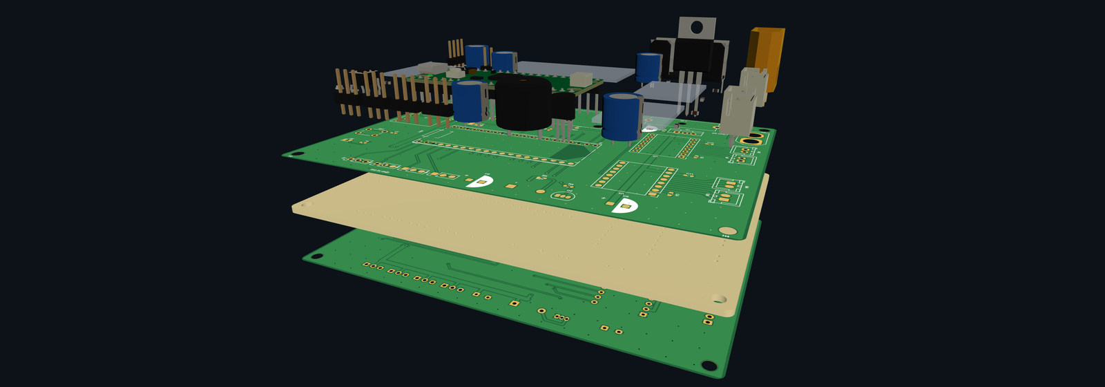
Checking a board in 3D catches mechanical mistakes before anything is made: a tall capacitor sitting under a plugged-in module, a connector facing the wrong way, or a barrel jack blocked by a mounting screw. The 3D view renders the board stackup, copper, solder mask, silkscreen and the 3D bodies of the parts.
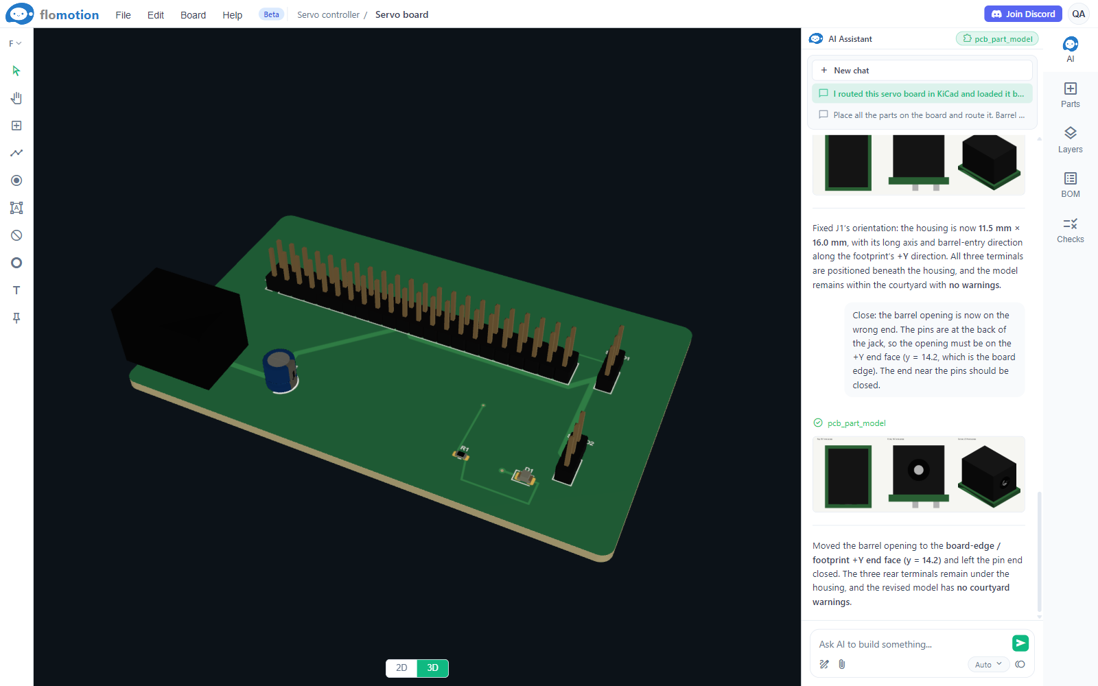
Standard parts pull their 3D shapes from the component library, but footprints for specific connectors or switches often have no 3D model attached. On the servo board, the CUI PJ-102AH power barrel jack had a footprint with pads and silkscreen but no 3D body. When a footprint lacks a model, the agent reads the footprint geometry and the part value, draws a 3D model to fit, checks its alignment against the footprint, and posts top, front and corner renders in the chat for inspection before placing it on the board.
When the layout is ready for manufacture, the editor also prepares a bill of materials formatted for JLCPCB assembly with LCSC part numbers. Modules and off-board parts such as development boards and motors are left out, and the agent asks in chat for any LCSC numbers it does not already have.
Limitations
A few constraints apply to typical board work:
- The PCB editor is in beta. Inspect the finished board in desktop KiCad and in the fabrication house's Gerber viewer before placing an order.
- Vias go all the way through the board; blind, buried and micro vias are not supported.
- Drawing a track by hand does not push existing tracks aside. Ask the agent to reroute a crowded area or move the neighbouring tracks manually.
- A 3D model drawn by the agent is an estimate from the footprint and part name. Check critical heights and overhangs against the manufacturer's datasheet before designing a tight enclosure around the board.
Summary
The FloMotion PCB editor turns a project schematic into a two- to 32-layer KiCad 10 board in the browser, combining manual layout tools with an AI agent that can place parts, route tracks, pour copper, run server-side KiCad DRC and build 3D models and assembly BOMs. It is built for moving breadboard prototypes onto solid, repeatable circuit boards and works alongside desktop KiCad on the same files.
Links
Try it yourself
Open the workspace, describe a part, and see what the agent does with it. No install, no setup. Sign-in is optional for the first run.
Start building