AI-generated schematics for KiCad
May 20, 2026
This guide covers the workflow from prompting an FloMotion AI agent for a schematic to opening that schematic in KiCad for PCB layout.
The basic loop
- Open a schematic editor with an AI agent.
- Describe the circuit. Include voltages, key parts, and topology hints.
- Iterate by chat until the schematic is right.
- Export to KiCad, open the project file, continue with PCB layout.
The handoff happens at the schematic. The agent does the rapid iteration; KiCad takes over for layout, where the tool quality matters more.
Writing the prompt
Concrete prompts produce concrete circuits. Useful things to specify:
- Voltages:
5V to 3.3V,12V to 5V at 1A. - Key parts:
AMS1117,ESP32,SK6812 LED. - Connections:
LED on GPIO 4,button on GPIO 0 with pull-up.
Example prompts:
A 5V to 3.3V regulator using AMS1117, with input and output decoupling caps.
An ESP32 dev board with a button on GPIO 0 and an SK6812 LED on GPIO 4.
A buck converter from 12V to 5V at 1A with input and output filtering.
Iterating
Edits are incremental. Common follow-ups:
Add a reverse-polarity protection diode on the input.
Swap the LED for a green one.
Add a 100µF bulk cap on the input.
The agent edits the existing design. Components and nets you've already placed stay where they are unless you ask for a change.
Annotating KiCad symbols before export
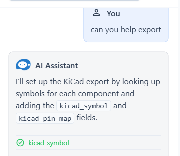
For the export to produce a usable netlist in KiCad, each component needs to map to a KiCad symbol from the standard libraries. Before exporting, ask the agent to look up and annotate the KiCad symbol for each part:
Look up KiCad symbols for every component and annotate them, or simply can you help export.
The agent searches the KiCad library by part name and assigns the matching symbol. For parts it cannot find, it falls back to a sensible common symbol (a passive resistor falls back to Device:R, an unknown IC to Device:U, and so on). The export still produces a valid project, and you can swap in a more accurate symbol in KiCad afterwards.
This step is important. Without the annotation pass, every component exports as a generic placeholder symbol. The schematic still opens in KiCad and the netlist is valid, but you lose the part-specific pin names, package shapes, and footprint hints, and you'll have to manually annotate every component in KiCad.
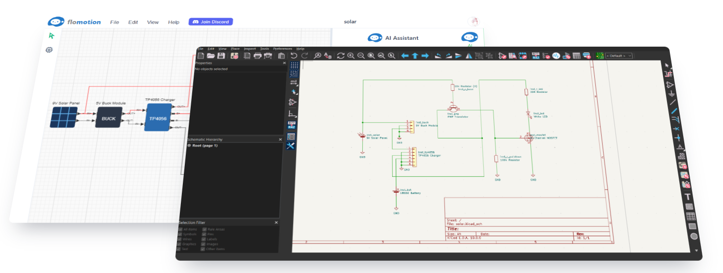
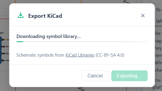
Exporting to KiCad
In the schematic toolbar:
- Open the menu, choose Export.
- Pick KiCad.
- The export downloads as a
.zipcontaining a KiCad project, schematic, and symbol references. - Unzip and open the
.kicad_profile in KiCad.
The schematic opens with components placed, nets named, and wires drawn. Power and ground use KiCad's power:GND and friends so the netlist resolves cleanly.
Wire routing is regenerated during export. KiCad symbols have different shapes and pin positions than FloMotion's, so the original wire paths no longer line up. The exporter re-routes each net against the new symbol geometry, so the netlist stays correct even though the wires look different from what you saw in FloMotion.
What carries over
Across the export:
- Component placements on the schematic canvas.
- Net topology: every connection becomes the right KiCad net.
- Power and ground: rails use KiCad's standard power symbols.
- Reference designators:
R1,C2,U1etc. are preserved. - Component values: resistance, capacitance, voltage ratings carry across when set.
Not yet carried:
- PCB footprints for arbitrary parts. Common passives (0603, 0805, SOT-23, SOIC-8, etc.) map automatically. Specialty parts need a footprint chosen in KiCad's symbol-to-footprint step.
- 3D models for parts. You can add them in KiCad after footprint assignment.
After the export, in KiCad
A typical follow-up sequence:
- Annotate if needed. Most exports come pre-annotated.
- Assign footprints for any specialty parts the auto-mapping didn't cover.
- Run ERC to catch anything weird that survived the export.
- Move to PCB: open the PCB editor and import the netlist.
Nothing about this changes how you use KiCad. The earlier stages just get done in chat.
Working with the agent
The agent is fast: you can get from a one-line description to a connected schematic in seconds. That speed comes with caveats worth knowing.
What to expect:
- Review the output. Results are often close to correct but can be wrong in ways that aren't obvious at a glance: a misread pin function, the wrong polarity on a tantalum cap, a missing pull-up. Read through the schematic before exporting.
- Watch for over-complication. The agent will sometimes add extra components when an existing part already covers the need, like a separate level shifter when the MCU pin is already 5V tolerant, or a discrete regulator when a dev board has one onboard. Prompt it back: the ESP32 board already has a 3.3V regulator, remove the LDO.
- Verify component choices. Specific parts (regulators, MCUs, sensors) are usually fine. Generic parts (resistors, caps) get reasonable default values, but recompute them for your case if it matters.
What the agent does not do:
- PCB layout. The schematic-level routing is for readability. PCB routing happens in KiCad.
- Design rules beyond the obvious. It does not run DRC or check for trace width / clearance issues. That is KiCad's job.
Treat the agent as a fast first draft, not a finished design.
Getting started
- Sign in and click Start Building.
- Create a project, then a new schematic.
- Describe the circuit in the chat panel.
- Iterate, then export to KiCad.
Try it yourself
Open the workspace, describe a part, and see what the agent does with it. No install, no setup. Sign-in is optional for the first run.
Start building